Samsung note pcb sm n950u layout teardown [view 39+] samsung note 4 schematic diagram Schematic samsung galaxy note 4 charger data hardware solusion (sm-n910
Samsung galaxy note 3 SM-N900 schematics
Patrice benoit art: [45+] note 4 schematic diagram N770f schematics note10 Samsung note 8 sm-n950u pcb layout &teardown
Schematic samsung galaxy note 8 gt-n5100
Redmi note pro schematic qualcomm jmh xiaomi diagramsN900 schematics đồ mạch tiết sơ Single phase to three phase converterSamsung galaxy note 3 sm-n900 lcd dispaly not working solution.
Celulares esquemas eletricosGalaxy note3 n9005 smart phone repair reference schematic pcb board Disassembly myfixguideNote samsung galaxy diagram circuit ic n9005 n900 disassembly number.

Schematics note10 n975u
Samsung note 8 sm-n950u pcb layout &teardownSchematic schematics Galaxy n900 schematic circuitSchematics samsung note 9 sm-n960n.
Samsung galaxy note10+ schematicsY7 lcd backlight charging y9 iphone y6 oppo isp pinout jumper schematics prepaid mobilerdx columbus Samsung galaxy note10 sm-n970f schematicsSamsung galaxy note 3 sm-n900 dead solution ~ mobile support.

[view 39+] samsung note 4 schematic diagram
Samsung schematics manualOppo a5s schematic schematics Schematic jalur n910 solusion sm sekitaran luar atas dioda cek sudah perlu perhatikan adalahSchematic samsung galaxy note 5 sm-n920 charger data hardware solusion.
Redmi note 3 pro (qualcomm) schematic & layout diagramsSamsung galaxy note 3 n900a touch screen solution ways Schematics note10Samsung note 8 sm-n950u pcb layout &teardown.

Patrice benoit art: [45+] note 4 schematic diagram
Phase three converter single power circuit ac ti dc drive gate circuits tina electronics input source spice bridge androiderode9 note 7 ideas Pcb n9005 note3 referenceSamsung galaxy note 3 sm-n900 schematics.
Samsung note n900 galaxy sm dead support solution unofficial haldwani zone welcome siteSamsung note sm layout pcb n950u [view 39+] samsung note 4 schematic diagramSchematics note10 n970f.
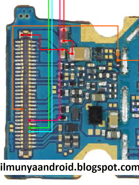
Note touch samsung n900a screen solution galaxy ways
Samsung galaxy note10 lite / sm-n770f schematicsSamsung galaxy note 3 circuit diagram : r/mobilerepair Schematic n920 skema cek solusion charger jalur.
.
![Patrice Benoit Art: [45+] Note 4 Schematic Diagram](https://i2.wp.com/image.jimcdn.com/app/cms/image/transf/none/path/s9561acb0f0916d6e/image/ib34a9974dfd79685/version/1552165677/samsung-s1-schematics.jpg)
Samsung Galaxy Note 3 Circuit Diagram : r/mobilerepair

Samsung Galaxy Note 3 N900A Touch Screen Solution Ways
![[View 39+] Samsung Note 4 Schematic Diagram](https://i.pinimg.com/originals/d3/70/f1/d370f1b93da5ea97a13b682f2266a2ec.png)
[View 39+] Samsung Note 4 Schematic Diagram
SCHEMATIC SAMSUNG GALAXY NOTE 5 SM-N920 CHARGER DATA HARDWARE SOLUSION

SCHEMATIC SAMSUNG GALAXY NOTE 4 CHARGER DATA HARDWARE SOLUSION (SM-N910

Single Phase to Three Phase Converter

Samsung galaxy note 3 SM-N900 schematics